What new applications are possible with BEX technique in SEM?
24th October 2024 | Author: Haithem Mansour
On October 31st, I will be hosting a webinar titled "Pushing the Boundaries of Microanalysis in SEM with the BEX Technique". In this session, I will share the new applications we have discovered since the development of the BEX technique in 2023. What exactly is BEX? What insights have we gained? Does BEX offer new applications, or is it merely a "fast and sensitive EDS" solution?
A new technology with new capabilities
A wise man once said, “with new technology comes new capabilities”. I can’t believe it is just over a year since we launched the Unity detector, and with it, the new BEX technique. It has been a crazy year, full of excitement during which I was busy introducing this new technique to the EM community around the globe and, at the same time, learning about the new capabilities it brings to SEM microanalysis and even nano-analysis.
It is great to see the level of awareness about this new technique in the EM community such a short time since its launch. Some techniques take years for awareness to develop, but it is fascinating how fast the news about BEX and Unity has spread and continues to spread. This has resulted in a rapidly increasing demand for Unity detectors! It is great to see Unity adopted on all continents around the globe and in some renowned institutions.
One of the most memorable moments of the year has been the recognition of Unity detector as one of the best ten microscopy innovations of the year in the 2024 Microscopy Today Innovation Awards. I had the honour to receive the award on behalf of all my colleagues at the end of July during M&M2024 in the USA. It is particularly gratifying to receive this recognition from such a well-respected organisation in the world of microscopy.
Figure 1: Microscopy Today Innovation Award presented to Oxford Instruments for developing the Unity detector
Revealing undiscovered secrets of your sample in 3D
During the past year, my colleagues and I have done well over 150 Unity demonstrations. It is fascinating and greatly motivating to witness EM experts’ reactions when analysing their samples with Unity for the first time! There is always a “wow” moment”, when it seems like they see their sample for the first time. Actually, what is happening is they are seeing it under a different “light” at a different speed and scale. Very often, they discover something totally new about the sample in just a few seconds or minutes. It could be a phase they never seen before or a fine structure they missed with other techniques; or sometimes they see that they can achieve in few minutes what they are currently sometimes spending days on.
Phases in granite
We learned that BEX offers a lot more than just a faster version of EDS. It is working in conjunction with EDS, enabling new capabilities and pushing the boundaries of microanalysis in the SEM. Figure 2 shows an example, where we compare fast imaging (at 5 fps) using BEX and BSE on a granite sample. Although BSE is great at detecting phases quickly, it has its limitations. In fact, the BSE noise increases when trying to separate phases with small Z-atomic number differences (<1). With such phases, one needs to scan very slowly and change contrast and brightness adequately to separate the phases. Therefore, detecting such differences during sample navigation using only BSE is impossible. In contrast, BEX allows the detection of such differences during high-speed imaging as it colours the image with elemental information, making it possible to detect such phases in just few seconds. This is demonstrated in Figure 2 with the calcium-rich phase, indicated with a white arrow, which is indistinguishable from the matrix in the BSE image but coloured in red in the BEX image (white arrows).
Figure 2: Comparison between (a) live BEX imaging and (b) Live BSE imaging at 5 frames per seconds on a granite sample. The data was collected simultaneously under the same conditions using a BEX detector.
In addition, one can note the limitation of the BSE signal to separate small and large atomic number differences at the same time. The zirconium-rich phase, indicated with red arrows, is saturated in the BSE image. Any phase with higher atomic number will also appear white and thus cannot be distinguished in the BSE image. BEX overcomes this limitation as it uses elemental information.
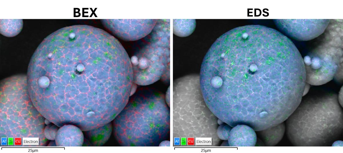
Elements in metallic powder
Figure 3 shows an analysis of a metallic powder used in additive manufacturing brought by a customer for BEX analysis at the Oxford Instruments Innovation Centre at High Wycombe. During the demonstration, the customer was very surprised to see the red structure (Cu-rich phase) in the BEX image as they had not seen when analysing the sample in their lab with EDS. After the demo they tried to detect the same feature again in their lab using the same conditions but failed. This is due to two main factors. Firstly, the sample is rough and unlike EDS, BEX is not affected by topography, so the BEX X-ray data does not suffer from shadowing as demonstrated in the figure. Furthermore, BEX is so sensitive that it can detect low concentration elements and tiny structures under optimum imaging conditions (low beam current). This enables mapping fine structures even if the concentration is low. The BEX map in figure 3 was collected in 30 seconds.
Figure 3: Comparison between BEX imaging and EDS overlaid on an electron image of metallic powder grains. The data was collected simultaneously under the same conditions.
Resolution on a semiconductor
Another example among the great things achieved with BEX is high resolution analysis using low kV or STEM mode. Figure 4 shows a STEM example of Unity on a semiconductor sample (lamellar prepared with FIB) where a resolution of < 10 nm is achieved.
Figure 4: Unity BEX STEM mode analysis of a semiconductor sample.
Scanning whole samples in minutes
To conclude I wanted to show an example of the Unity Cartography mode, which takes advantage of the imaging speed and scans a whole sample in an automated way. This is real-time analysis; the video is not accelerated.
In summary
What we learned during this past year emphasises that the Unity detector and the BEX technique is not only for elemental imaging but also for micro and nano-analysis. It is ideal for easy-to-use, routine analysis, and it is pushing back the boundaries of what can be done in an SEM.
Join me in my upcoming webinar where I will showcase more exciting applications with BEX.
Dr Haithem Mansour,
BEX Product Manager, Oxford Instruments
Dr. Haithem Mansour graduated with a PhD in Material Science from the University of Lorraine in France. He joined Oxford Instruments in 2016 and has always worked with a strong focus in electron microscopy and microanalysis. Haithem has focused his research in ECCI, EBSD and EDS, in particular the development and improvement of these analytical techniques. He is currently working as BEX/EDS Product Manager within the NanoAnalysis marketing team, where he helps design, develop and market new analytical systems.