When it comes to in situ FIB lift-out, there are many things to consider, one aspect which is often overlooked is the grid you attach your lift-out sample too. The majority of FIB users use a standard grid. This is inevitably copper, usually with 3 posts. However, there are many alternatives available with different materials and designs, each with its own advantages.
How many posts?
The number of posts on a grid is primarily an indication of how many samples you can attach - more posts, more samples (but narrower posts). Some prefer not to attach multiple samples to a single grid, to minimise the risk of damage when manually handling the grid. However, the use of multiple post grids can be advantageous, as they give a redundancy against damaged/misaligned grids and samples lost due to over-thinning. There are 2 post designs: flagpole and V notch. Each is suited to different attachment methods and applications.
1. Flagpole: attaching to the side of either post is a common approach due to its simplicity and speed, it is ideal for plan-view samples or when EDS is desired. Although some samples may be prone to warping during thinning and TKD analysis can suffer from shadowing from the grid post.
2. V-notch: the middle position can be used for both small and large samples. It is ideal for mechanical stability and creating thin samples since both ends of the sample are attached. However, redeposition of the grid material onto the sample may occur during thinning, so this location is not ideal for EDS. As the sample is on top of the post, shadowing which can occur on a flagpole sample during TKD analysis is not an issue.
3. Tomography: welding to the top of a post or grid finger can be used for 3D (FIB and X-ray) tomography and atom probe tomography (APT).
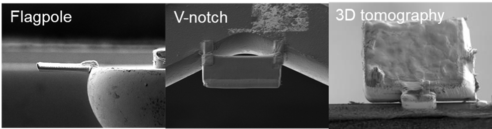
Examples of common lift-out attachments for FIB and P-FIB
Copper Grids
Copper grids are the most popular because they are relatively inexpensive and offer a smooth surface for attachment. They also provide flexibility for different attachment approaches with their different post designs. Being copper and <50 μm thick, they do need care when handling. There are 2 variations of most Cu grid designs, created by different manufacturing processes (identifiable by the downset value of the Cu grids). Visually both grids are similar (see photo below), but the sharpness of the edges commonly used for attachment are different (see electron image of the V post from each grid, the difference is most noticeable at the base of the post), while both are suitable for lamella preparation the more defined shape simplifies the process.
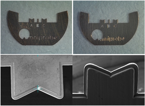
Left “Standard” grid compared to right a “shallow downset” grid
Molybdenum Grids
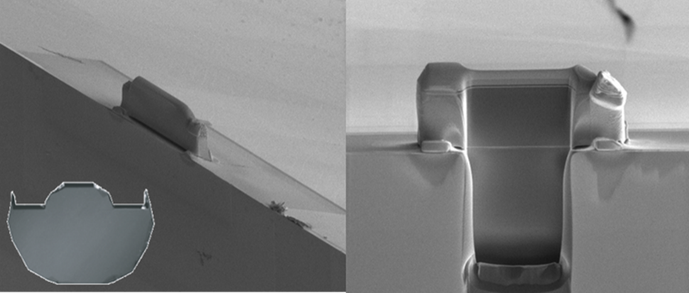
Molybdenum grids are similar in design to the Cu grids (available in 3-post and 4-post configurations) and are suited for EDS analysis of Cu-containing samples. These grids are challenging to fabricate and present a more textured surface compared to the Cu grids. In some cases, you may need to FIB mill small burrs to achieve a smooth, flat attachment surface. Using the 3-post grid when a V post is required can be beneficial, as v notch on a 4-post grid is shallow, as seen below.
Images of 3 and 4 post Moly grids
Beryllium Grids
Beryllium provides the lowest background EDS signal. However, fabrication is limited due to the material’s properties, which make it problematic to work with, as such these grids are only available as a half ring.
Silicon Grids
The final grid available is Silicon. Silicon grids are ideal for silicon semiconductor devices, as the grid mills at the same rate of the device matrix and introduces no additional elemental contamination. They are significantly different from traditional OmniGrids. There are 2 main designs, bevelled and shapable fingers. As silicon mills quickly, the finger design is intended to be customised to match your sample and application; atom probe tomography is a good example. The bevel design is angled to match the angle of a conventional undercut. This provides a fast, simple way to attach a sample by multiple points (see advantages of the V-notch). The grids are ~ 100 mm thick, which makes them more rigid compared to metal grids and easier to handle - particularly important for cryo applications. The removal of the fingers on the bevelled grids also benefits cryo, as the deposition used to attach the sample is not shadowed by the grid post.
Bevelled silicon grid, shows matched milling rate to silicon wafer sample attached
Hopefully, this brief introduction has given you valuable insight into the value of each of the different grid types and will allow you to select the best grids for your needs. You will find a variety of options to suit every application available from our e-store.