Using Wavelength Dispersive X-ray spectroscopy (WDS), scientists can perform elemental and chemical analysis of samples with a scanning electron microscope (SEM), focused ion beam (FIB) SEM or an electron microprobe (EPMA). Oxford Instruments' WDS detectors use the AZtecWave software package, a materials characterisation software that facilitates research at the micro and nanoscale.
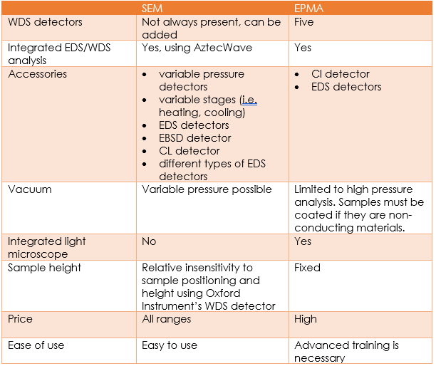
An EPMA is nearly identical to a SEM but differs in chamber construction. An EPMA is purposely built to enable mounting multiple WDS detectors that facilitate quantitative chemical analysis at high sensitivity, whereas a SEM chamber is built to enable mounting different detectors. EPMA chambers are more limited in configuration because of the multiple, large WDS detectors. Having multiple detectors on the same instrument is beneficial, as it allows simultaneous collection of different elements.
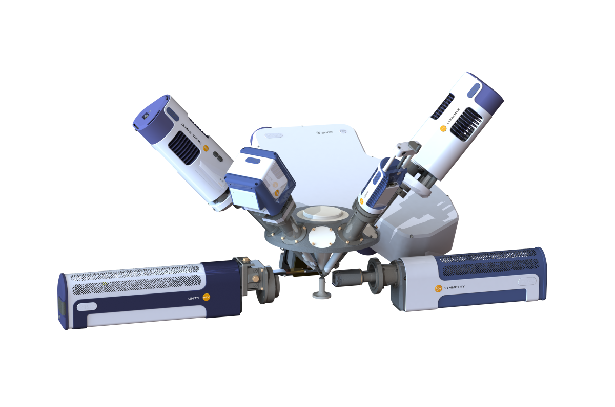
EPMAs commonly have an array of imaging detectors (SEI, BSE, and CL) that allow the investigator to generate images of the surface and internal compositional structures that help with analyses. SEMs often have different equipment; variable pressure SE and BSE detectors, EDS detectors, EBSD detectors and different stages for varying experiments (heating/cooling, tensile and compression stages, etc.) as seen in figure 1.

Figure 1. A dummy configuration of different Oxford Instruments detectors mounted on a scanning electron microscope, including a 170 mm² EDS detector, a windowless EDS detector, an OmniProbe manipulator, a Symmetry EBSD detector and a WDS Wave detector.
Vacuums are standard in all electron microscopes. EPMAs are held under high vacuum to prevent gas and vapour molecules from interfering with the electron beam on its way to the sample. SEMs come in all different configurations. Some SEMs are variable pressure microscopes that allow users to work at variable pressure thereby decreasing the need to coat samples. Coating can be considered destructive; it therefore eliminates the possibility of analysing a sample using a different analytical technique in the future. EDS analysis of uncoated samples at variable pressure can successfully be carried out in a SEM but is not possible in an EPMA where the vacuum is fixed.
Unlike SEMs, EPMAs are equipped with a light microscope which allows for direct optical observation of the sample and for verifying sample height.
The Oxford Instruments WDS Wave detector is mounted on the SEM column at an inclined geometry. This presents an advantage to a WDS detector on an EPMA, as it broadens the plane of the Rowland circle, meaning that WDS analysis using the Wave spectrometer is less sensitive to sample positioning and height. Unlike a vertically mounted WDS detector on an EPMA (which is sensitive to sample position), WDS analysis using a Wave detector is quick and easy, as sample height/position is not the most critical factor. Oxford Instruments is the only WDS detector manufacturer for SEMs with a Rowland circle. Parallel beam WD spectrometers are more sensitive to sample height. The AZtecWave software combines the high spectral resolution of the Wave Spectrometer, to resolve X-ray peaks and quantify minor and trace elements, with the speed and flexibility of EDS. This delivers an advanced and complete solution for compositional analysis on the SEM.

As already indicated, an advantage of a SEM over an EPMA is that different types of detectors can be mounted on a SEM. Now let’s discuss detectors commonly associated with electron microscopes:
- EDS analysis provides elemental and chemical analysis of a sample inside the SEM, TEM, FIB or EPMA.
- While EPMA’s are generally reserved for high sensitivity quantitative analysis, meaning most ports are taken by the WDS detectors. SEMs often have ports of various sizes available for EDS detectors (which have a smaller exterior footprint).
- Oxford Instruments manufacturers a variety of EDS detectors; some with windows for standard/fast analysis and some windowless for the analysis of nanoparticles or light elements.
- Different kinds of EDS detectors will most likely be found on a SEM
- EBSD is a scanning electron microscope (SEM) based technique for materials characterisation. In EBSD, the electron beam is scanned across the surface of a tilted crystalline sample; the diffracted electrons at each point form a pattern that can be detected and then analysed using dedicated hardware and software. At each point, the indexing process provides information about the phase and the crystallographic orientation from which the microstructure can be effectively reconstructed. EBSD is unique to SEMs as the sample stage cannot be tilted in an EPMA.
- Backscattered Electron and X-ray (BEX) Imaging combines backscattered electron and X-ray signals to deliver rapid high-definition colour images embedded with elemental data. The detector is located directly beneath the pole piece to maximise signal collection, ensuring it can be used at normal imaging speed and operating conditions, making imaging elementary.Cathodoluminescence (CL) is the emission of visible light when an electron source interacts with a sample. CL detectors are often found on EPMA’s and help reveal sample properties that are not otherwise visible using an optical microscope, secondary electron (SE) detectors or backscattered electron (BSE) detectors. CL detectors can also be mounted on a SEM and are useful on electron microscopes because they help scientists better understand the composition, growth and photoemission properties of a material.
WDS spectrometers are often found on scanning electron microscopes and heavily used on EPMAs. To find out more about WDS or to schedule a demonstration, contact an Oxford Instruments applications specialist.


