8th September 2021 | Author: Dr Rosie Jones
Recently, we launched new functionality in the AZtecWave software – WDS Scan. I am excited to share this development, as it harnesses the high resolution of the Wave spectrometer and allows its capability to be shown with an easy-to-digest, visual result.
The Wave spectrometer is the only WDS solution for the SEM with a fully focusing Rowland circle geometry and curved crystals. The design is very similar to that of WDS spectrometers used on electron microprobes, and consequently provides a similar level of spectral resolution. High spectral resolution is the key benefit the Wave spectrometer brings to the analytical SEM – the resolution is usually >10x higher than can be achieved using EDS.
This enables closely occurring X-ray lines, and all the common peak overlaps that occur in the EDS spectrum (e.g., Cr/Mn, Fe/Co, Ba/Ti, S/Pb, and the REE), to be fully resolved. The Wave spectrometer is also the only WDS solution for the SEM that can fully resolve challenging overlaps such as S Kα/Mo Lα and Ti Kβ/V Kα. As a WDS Scan measures the counts generated at stepped positions over a defined energy range, it produces a visual result that can be directly compared to an EDS spectrum.
In this post, I will show, using several different sample types, the capability of AZtecWave and the Wave spectrometer to resolve challenging X-ray peak overlaps and to positively identify the presence of (trace) elements in samples.
Overlapping S and Mo lines
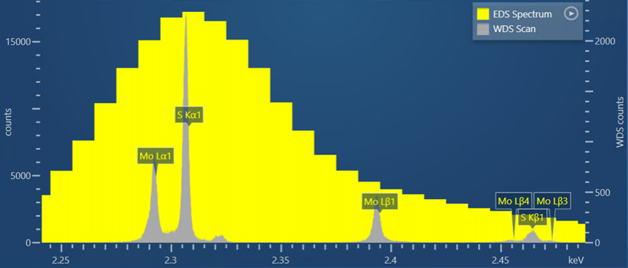
This first example is of the overlap between the S Kα line, at an energy of 2.307 keV, and the Mo Lα line, at an energy of 2.293 keV. Here, we observe this overlap in a S and Mo bearing mineral called Molybdenite (MoS2). The yellow spectrum in Figure 1 is the EDS spectrum collected for the molybdenite – in this, it is not possible to differentiate the S and Mo peaks. In comparison, the grey spectrum in Figure 1 represents a WDS scan. Here you can see that the S and Mo peaks are clearly separated and distinct, giving certainty to the presence of these two elements and enabling accurate quantitative measurements to be made.

Figure 1. A WDS scan obtained from a sample of molybdenite shown alongside an EDS spectrum collected for the same sample.
AZtecWave contains unique technology to help set up the WDS scan collection settings. It automatically selects the optimum crystal, slit size and slit position for the WDS scan based on the SEM-system conditions and the sample composition. The WDS scan shown in Figure 1 was collected using these ‘Auto’ options selected by the AZtec software.
Overlapping Ti and V lines
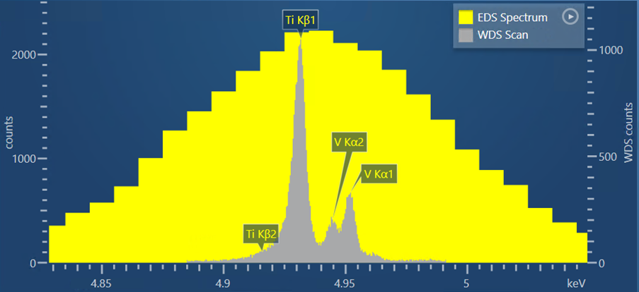
Another sample I have analysed using WDS scan in AZtecWave is a Ti-6Al-4V alloy. My reason for choosing this is there is a close overlap between the Ti Kβ peak and the V Kα peak which occurs at energies of 4.931 and 4.494, respectively. Figure 2 shows a WDS scan produced by the Wave spectrometer and AZtecWave.

Figure 2. A WDS scan obtained from a Ti-6Al-4V alloy, shown in comparison to the EDS spectrum obtained for the same sample.
For this scan, I used the automatic selection of crystal and slit position, but I tweaked some of the other collection settings from the ‘Auto’ options. I did this based on the theoretical WDS scan that is shown in the setup step (i.e. prior to acquisition), which shows what the experimental WDS scan is likely to look like using the current collection settings. If the settings are changed, then AZtec will recalculate the theoretical WDS scan – this is extremely useful for further optimisation of the scan settings and removes the need for lots of trial-and-error scans.
Based on what was shown in the theoretical WDS scan, I increased the dwell time to 1000 ms to reduce the noise and produce a very high quality WDS scan. In the resulting scan, it is not only possible to see the separation of the V Kα1 peak from the Ti Kβ peak, but also the V Kα2 peak.
Detecting trace elements
As part of this recent AZtecWave development, we have also optimised the actual movement of the Wave spectrometer (needed to perform a WDS scan) so that it is able to scan at a slower speed than was possible with our previous generation of software (Inca Wave). Dwell times of up to 50 seconds per step can now be selected to perform very slow scans, which are likely required to detect trace elements.
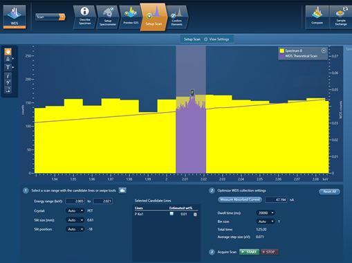
My final example demonstrates this – it is a scan for trace P (~100 ppm) present in a steel sample. Figure 3 shows the setup of the WDS scan in the AZtecWave software. The P Kα line has been entered as a candidate-element line with an estimated wt.% of 0.01. All the settings for this WDS scan have been automatically selected by the AZtecWave software, except for the dwell time, which I manually changed to 20,000 ms. The WDS theoretical scan with these settings can be viewed in the spectrum viewer (in purple) and shows that a small P peak should be identifiable in the scan.

Figure 3. A snapshot of the AZtec software showing the settings used for scanning trace P in a steel sample.
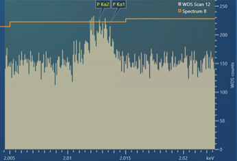
The resulting experimental scan, using the settings shown in Figure 3, is shown in Figure 4. As you can see, the experimental scan is very similar to the modelled, theoretical WDS scan shown in Figure 3 – showing that the theoretical WDS scan in AZtecWave gives a good prediction of what a resulting scan might look like.

Figure 4. A WDS scan obtained for the P Kα peaks present in a steel sample containing ~100 ppm P.
I hope I have been able to show you the enhancements brought by the Wave spectrometer and the new functionality available in AZtecWave for clearly separating peak overlaps and positively identifying the presence of elements, including trace elements, present in a sample. If you would like to know more, please join me for a tutorial and live Q&A session on the 15th September.


